|
All times refer to time zone CET
|
Klick title to show / hide detailed session description
|
08:15
A5
|
|
Opening
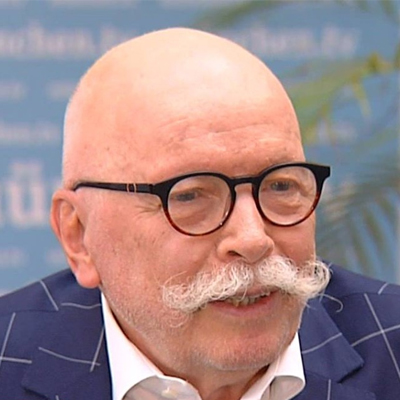
- Roland R. Ackermann
- Correspondent Editor Bavaria
- Bodo’s Power Systems
- (No session description available yet)
|
08:30
S1
|

|
Silicon Carbide JFETs enable breakthroughs of high-voltage solid state power distribution
- Leo Aichriedler
- Distinguished Engineer Application Marketing
- Infineon Technologies
- New, emerging low-voltage (< 1000VAC and < 1500VDC) power distribution schemes require fast-acting circuit protection devices, which are typically implemented as solid-state circuit breakers (SSCBs). Unlike conventional electromechanical breakers, SSCBs comprise semiconductor power switches enable the interruption of faulted circuits within sub-µs range. The employed power switch has to support low conduction losses during normal operation while also being capable to handle extreme overvoltage and overcurrent / short-circuit events in a reliable manner. To meet these specific requirements, Infineon Technologies has developed an application-tailored Silicon Carbide JFET technology that enables ultra-low RDSon (1mΩ - 5mΩ at 750V - 1.2kV VBDss) power devices in standard discrete packages. Starting from key requirements of SSCB applications, the presentation focuses on the specific features of the new JFET technology and demonstrates its performance using practical application measurements.
|
08:45
S2
|

|
Paralleling SiC MOSFETs: A Robust Approach for High-Power Converter Performance and Thermal Management
- Salvatore La Mantia
- Technical Marketing Manager
- STMicroelectronics
- As multi-kW converter designs increasingly rely on Silicon Carbide (SiC) MOSFETs, paralleling discrete devices becomes essential to achieve necessary current and thermal capabilities. Despite potential engineers’ hesitation, this presentation demonstrates that proper techniques allow parallel SiC MOSFETs to significantly boost converter performance and design flexibility.
|
09:00
S3
|

|
Innovative SiC MOSFET Technologies for a wide range of applications
- Dr. Khalid Hussein
- Senior Manager Power Semiconductor, Technical Marketing Automotive
- Mitsubishi Electric
- Mitsubishi Electric is steadily promoting innovative SiC MOSFET-based power device solutions for a wide range of high-reliability, high-efficiency, and demanding applications. The launch of a new highly automated 8-inch SiC processing facility is also proceeding as planned. (Production is scheduled to start within 2026). In this presentation, we will show our in-house designed and developed efficient SiC MOSFET bare dies (both planar and trench) and compact, highly reliable transfer mold packaging technology. Presentations highlight unique structures and the performance (Rdson, short-circuit capability, switching loss) that lead to trade-off optimization between devices, as well as promising recent achievements in proton implantation technology. It also provides examples of power modules for automotive and consumer applications.
|
09:15
S4
|

|
Selection and Optimization of Topside Cooling Options for Discrete SiC MOSFETs for High Power Density Applications
- Dr. Tomas Krecek
- Senior Field Application Engineer
- Alpha and Omega Semiconductor
- A major benefit of wide bandgap devices is the ability to significantly increase the power density of the system. Whether the application is a smaller, lighter on-board charger or a slim PSU in an AI server rack, designers are turning to topside air or water cooled power devices with increased thermal dissipation to further extract the benefits of SiC MOSFETs. In this talk we will review the major SiC MOSFET discrete topside cooled package options and discuss the differences and best practices when selecting and optimizing for your design.
|
09:30
S5
|

|
Design and Reliability Considerations for 3.3kV SiC Modules in Traction
- Dr. Virgiliu Botan
- Senior Product Manager BiMOS
- Hitachi Energy
- SiC Modules are making their way into conservative applications like Traction due to their unbeatable reduction of switching losses. For a DC-DC converter this allows the system designer to massively reduce the size of the inductor by operating at increased frequencies. Nevertheless, concerns are raised about the cost and reliability of such novel modules. This work will explore some of the challenges associated with ensuring decades of lifetime in a challenging environment.
|
09:45
B1
|

|
Coffee Break & Tabletop Exhibition
-
-
-
- All breaks and catering, as well as the tabletop exhibition, will take place in the foyer.
The perfect spot for networking and learning about the latest products and services!
|
10:30
S6
|

|
Increasing power density with small molded modules in medium power applications
- Dr. Christian Felgemacher
- Director Application Engineering
- ROHM Semiconductor
- Transfer molded half-bridge modules with SiC MOSFETs are already available and established for use in high power converters of above 100 kVA such as xEV traction inverters. Additionally, for power conversion stages of not much more than 20 kVA solutions exist in the form of HSDIP20 modules with 4-in-1 or 6-in-topologies, which offer great alternatives to discrete devices for creating compact and highly integrated designs. For medium power applications between these power areas device paralleling is often required. To close this gap ROHM has developed the compact DOT247 module. In this presentation the package will be introduced and its benefits, such as reduced commutation loop inductance as well as improved heat dissipation will be discussed along with usage options in target applications such as datacenter power supplies or charging infrastructure.
|
10:45
S7
|
|
SiC semiconductors in space applications: trends, challenges and opportunities
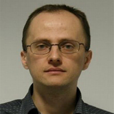
- Dr. Darko Vračar
- Power Electronics Senior Engineer
- The Exploration Company
- Recently we are witnessing a move from turbochargers towards electricpump-fed systems in rocket engines and many companies entering the space business. The presentation will start with short introduction of liquid-fuel rocket engines and their electrification trends. Then power electronics related topics like choice of semiconductors, high altitude and vacuum operation, radiation hardness, partial discharge, and cryogenic aspects will be covered. Also, practical tips and challenges for hardware development engineers will be presented as well as opportunities for semiconductors’ manufactures.
|
11:00
S8
|
|
Advanced SiC technology for automotive applications
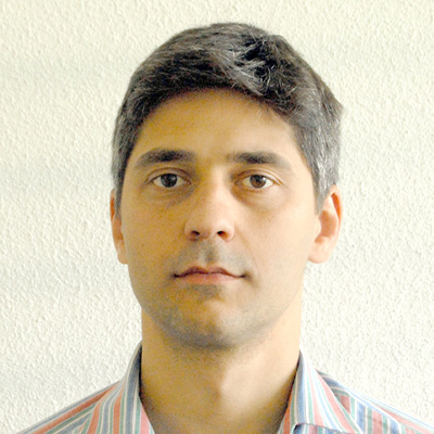
- Dr. Andrei Mihaila
- Director SiC Mosfet Design
- StarPower
- StarPower is a relatively new player in the SiC market, however present with a proven track record of automotive designs already in mass production. In this presentation, we will provide an overview on our SiC program and product platforms for various market types. We will explain why we see a future for planar technology for the next product generations and discuss key design considerations in terms of performance and reliability requirements, detailing how these market requirements translate into practical Mosfet design considerations.
|
11:15
S9
|

|
Accurate Efficiency Analysis for WBG inverters: Confidently Capturing 0.1% Improvements
- Roy Hali
- Senior Application Engineer
- HIOKI
- Engineers working with WBG semiconductors in their designs need measurement solutions to validate efficiency gains that simulations promise. Since these efficiency gains can be as small as 0.1%, accurate and repeatable test results are a must. Wide bandgap semiconductors such as SiC and GaN are driving the next generation of power conversion systems. Their superior material properties enable higher switching frequencies, lower losses, and conversion efficiencies that often exceed 98%, clearly surpassing conventional Si-based devices. While these advantages allow more compact, lighter, and more efficient designs, they also introduce new measurement challenges. High switching frequencies, fast transients, and reduced loss levels make it increasingly difficult to capture accurate data with conventional approaches. In this presentation, we will discuss these challenges and showcase HIOKI’s advanced solutions for precise and reliable evaluation of conversion efficiency under high-frequency and high-efficiency operating conditions.
|
11:30
S10
|
|
Efficient and Reliable 2kV SiC Power Modules for DC Infrastructure and Renewables
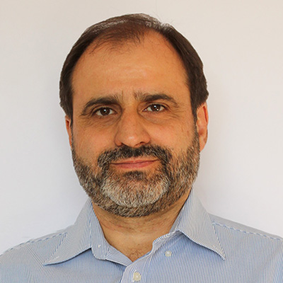
- Dr. Jorge Mari
- Senior Principal Engineer
- Semikron Danfoss
- With the objective of reducing direct current and associated conductor sizes, many applications have seen an incrase in the DC link voltage to up to 1500V. This is the case for utility-scale solar farms, Energy Storage Systems, electrolyzers for Hydrogen production, High Power EV chargers, Trucks and Off Highway Vehicles. With these applications in mind, all of which require a high reliability product, Semikron Danfoss has developed a 1700A 2kV SiC power module which is now in series production. The module exhibits a fantastic 0.8 mΩ forward resistance and thanks to its careful chip-layout exhibits stable text-book switching waveforms in all its voltage, current and temperature range. Through extensive qualification tests at chip and module level the module is best prepared for applications requiring reliable long life performance. In this talk we shall illustrate some of these features comparing its advantages over higher voltage modules.
|
11:45
S11
|

|
Comparative Analysis of Power and Thermal Performance in SiC MOSFET SMD Packages: X.PAK, QDPAK & D2PAK-7
- Fatih Cetindag
- SiC Principal Power Application Engineer
- Nexperia
- This presentation provides a detailed evaluation of SiC MOSFET discrete packages, focusing on thermal and electrical performance differences between top-side-cooled and bottom-side-cooled architectures. It compares three key packages: D2PAK-7, X.PAK, and QDPAK. A major finding is that the top-side-cooled QDPAK and X.PAK packages support significantly higher power levels than the bottom-side-cooled D2PAK-7. This is due to their superior thermal management: top-side-cooled devices dissipate heat directly from the top of the package to a heatsink via a thermal interface material, decoupling thermal and electrical paths. In contrast, D2PAK-7 relies on PCB-based heat dissipation, which limits its thermal performance. The analysis also shows that top-side-cooled packages offer lower parasitic loop inductance and enable higher power density and peak efficiency, especially under continuous high-load conditions. The presentation concludes with design recommendations, emphasizing the importance of selecting a package architecture that co-optimizes thermal and electrical performance to fully exploit the advantages of SiC technology in advanced power applications.
|
12:00
B2
|

|
Lunch Break & Tabletop Exhibition
-
-
-
- All breaks and catering, as well as the tabletop exhibition, will take place in the foyer.
The perfect spot for networking and learning about the latest products and services!
|
13:45
S13
|

|
The Application of Miniature Planar Gate Drive Transformers
- Dr. Rosemary O’Keeffe
- Senior Application Engineer
- Bourns
- Modern power conversion techniques have been evolving to towards ever increasing speed and efficiency as part of the electrification revolution of recent years, driven by industries such as solar and automotive. Recently developed semiconductor technologies (SiC, GaN) help enable these technologies, but they do require careful design of the supporting circuitry to optimize their features. A key part the power conversion system is the driving of the semiconductor switches at its heart, that is the gate drive subsystem. The gate drive subsystem produces its own isolated power supply and the most critical component of this is the transformer. In this presentation we will evaluate the performance of a family of miniature high isolation high power density planar transformers made by Bourns.
|
14:00
S14
|

|
Beyond the FET: Solving the Practical Challenges of SiC Gate Drive Design
- Karsten Düchting
- Senior Strategic Marketing Manager High Voltage Power Products
- Allegro MicroSystems
- While much of the industry’s focus is on the SiC FET itself, experienced designers know that system performance is often dictated by the practical challenges of the gate drive circuit: component count, EMC robustness, and supply chain flexibility. This session moves beyond the FET to focus on solving these critical, real-world issues. We will introduce Allegro’s AHV85003/043 chipset and demonstrate how its key features - including an integrated bias supply and low common-mode capacitance - provide a streamlined path to creating robust, cost-efficient, and production-ready SiC power systems.
|
14:15
S15
|

|
SiC MOSFET Gen 2.0: Rugged in Radiation, Softer in switching
- Hadiuzzaman Syed
- Technology Performance Architect
- Bosch
- At Robert Bosch, the development of our cutting-edge SiC MOSFET trench technology is intrinsically linked to our robust vertical integration strategy. This approach ensures that each new generation of SiC MOSFETs is meticulously optimized to excel under the most demanding conditions of automotive applications. Our Bosch SiC Gen 2.0 delivers not only exceptional performance with optimized on-state resistance (RDS,on) but also boasts a softer switching behavior and superior robustness against cosmic radiation. Looking ahead, our transition to 200mm wafers guarantees that all future Bosch SiC MOSFET generations will continue to set industry standards for cost-effectiveness, performance, and unwavering reliability.
|
14:30
S16
|

|
Performance and Reliability Gains in MVHV SiC Using Advanced Power Devices and Packaging Technologies
- Sascha Dern
- Vice President Sales, EMEA & India
- Navitas Semiconductor
- Critical infrastructure upgrades in power grids, data centers, and renewable energy are driving new standards for longevity and resiliency in power semiconductors. To address these requirements, a novel trench-assisted planar SiC MOSFET technology is being deployed to support over 20 years of continuous operation. Further, advanced press-fit power modules, using epoxy-resin potting, provide protection against moisture and thermal stress. The final result is stable, reliable performance for infrastructure where failure is not an option.
|
14:45
B3
|

|
Coffee Break & Tabletop Exhibition
-
-
-
- All breaks and catering, as well as the tabletop exhibition, will take place in the foyer.
The perfect spot for networking and learning about the latest products and services!
|
15:30
S17
|

|
Benefits of 3-level power modules in Automotive traction inverters
- Sebastian Pawusch
- Application Engineer Automotive
- Fuji Electric
- Today’s BEVs predominantly use 2-level Voltage Source Inverters for traction, moving from IGBT based inverters to SiC-MOSFET based inverters. Inverter efficiency has greatly enhanced with the use of SiC, but system losses, EMI emissions can still be improved. PWM harmonics from 2-level inverters add copper, iron and rotor stray losses, causing heat in the electric machine limiting the constant output power. For most motor types used in traction their efficiency is limited when using 2-level inverters. Continuous increase in battery voltage and faster devices increase common mode disturbance and dV/dt, causing insulation and bearing stress. 3-level T-type inverters halve device switching voltage, enabling lower switching losses or higher switching frequency. Consequently, their output waveform closer resembles a sinusoidal waveform, lowering THD and current ripple. Additionally, dV/dt and common mode voltage are reduced, therefore lowering insulation stress and EMI emissions. Overall lower current ripple on the machine side improves its efficiency significantly.
|
15:45
S18
|

|
Assessing the aggregate behavior of paralleled SiC Mosfets
- Andrea Vinci
- Senior Technical Marketing Manager
- Tektronix
- Tektronix will present the critical factors affecting current sharing in paralleled SiC Mosfets configurations, in particular when it’s needed to determine potential imbalances causing devices to overheat or fail prematurely
|
16:00
S19
|
|
Next-Gen Motor Drives : Exploring SiC
- Dr. Didier Balocco
- PSG EMEA Marketing
- onsemi
- SiC for Motor Drive : When does it make sense? The International Energy Agency (IEA) estimates that motors are responsible for more than 45% of the world’s total electricity. Thus, finding ways to maximize their operational efficiency is paramount. The use of WBG materials, such as Silicon Carbide (SiC), allow those devices to outperform their Silicon (Si) equivalents. Higher efficiency drives, using SiC, can be smaller, more reliable and can reduced cost of ownership.
|
16:15
S20
|

|
Selecting the Right SiC MOSFET Device: A Key to Efficient Zero-Voltage Switching
- Dr. Ajay Poonjal Pai
- Head of WBG Innovation
- Sanan Semiconductor
- Zero-voltage switching (ZVS) in a power converter is a key technique for reducing switching losses, thereby enabling higher switching frequencies. ZVS is achieved by minimizing the voltage/current overlap during switching transitions through circuit parasitics or small passive-reactive components. This work investigates today’s leading 1200V SiC power MOSFETs under ZVS in a half-bridge up to 350kHz, providing clear device-selection criteria for designers of ultra-efficient, high-density soft-switching converters.
|
16:30
S21
|

|
Going Beyond a Qualification Report: Power Cycling and Lifetime Modeling
- Mauro Ceresa
- Senior Technical Director for EMEA and India
- Wolfspeed
- The electrification of transportation, renewable energy integration, and industrial automation place unprecedented demands on power semiconductor modules. Reliability, durability, and lifetime prediction are paramount, particularly in automotive and industrial applications where failure is not an option. This presentation will provide insights into power cycling and lifetime modeling approaches as a preamble for predictive maintenance.
|